
A while ago, I stumbled onto this blog post by Alexandru Groza that described the author’s journey to build their own 80386 single-board computer. It felt insurmountable to tackle such a project – while I have in the past successfully repaired simpler computers (like Commodore 64s), an entire computer build from schematic through to running real code felt out of reach.
I had good reason for it to feel out of reach, too. In the past, I designed some schematics and had PCBs manufactured by OSH Park. These were simple designs to add custom options to my selection of audio engineering equipment. These were as simple as a little diode clipper and even included a low-cost preamp. However, they often did not work! It was difficult to justify continuing to invest time and money into designs that were faulty from the outset.
Fast forward a few years. I had read a few more books, learned a thing or two. I designed some simple schematics and had them built by PCBWay for a fraction of the cost I had previously been paying. This time, drawing on a much better foundation of knowledge, these designs actually worked. Sure, there were mistakes and errors in the schematics and PCB layouts. But crucially, these mistakes were not fatal and could be easily worked around (and fixed in later revisions).
At the same time, I saw products like the Commander X16 gain traction and found myself fascinated by single-board computers like the Feertech MicroBeast. While I was intrigued by the computers themselves and the effort taken to build and release them, these all had the same problem for me: they were nostalgic for a different era than I’m nostalgic for. The computing era I’m most nostalgic for is the one I grew up in, messing with MS-DOS and early Windows. I understand the appeal of the Z80 or 6502 CPUs and computers like the Apple II or TRS-80. I own three Commodore 64s, each of which I have taken the time to repair to full functionality1.
I stumbled on the datasheets for the Intel 8088 CPU, and something finally clicked. It looked familiar, like the 6502 or Z80 in the other computers I was fascinated by. Inspired by the story of Alexandru’s 80386 computer, I finally knew I wanted to build a computer around the 8088 for myself. Further reinforcing the viability of this project, I learned about the Book 8088, a custom laptop built around the 8088 CPU. If they could do it, so could I.
I’ve done enough projects to know to set a clear target to avoid the temptation to infinitely iterate, so I set a clear goal: it had to allow me to play a full game of Sid Meier’s Civilization.
I recognized that achieving this goal would require PC compatibility. I elected to compromise on designing certain elements: for example, I would have an ISA bus for expansion cards to support disks and video graphics, rather than trying to build those circuits myself. With that decision in mind, I focused on building something that would fit into a common ATX case, just like any other motherboard you might buy today.
The rest of this post will dive deep into the journey, but if that feels like a lot of reading… in summary, it worked.
I have built my own computer on which I can play Civilization.


The First Prototype
I chose to implement my computer around the 8088 CPU rather than the very similar 8086 CPU primarily because the 8088 has an 8-bit data bus, and I imagined that would simplify the PCB layout. Running the CPU in “minimum mode” also simplified my design, at the cost of being unable to ever add a floating-point coprocessor to the computer. This also meant that reference materials such as the IBM 5150 PC technical reference manual were only partially helpful in validating my own design: those PCs ran the CPU in “maximum mode” to allow for coprocessors, so the signals weren’t a perfect match.
A fully PC-compatible computer has a wide range of devices on the motherboard itself. These include programmable timers, interrupt controllers, DMA controllers, keyboard and mouse controllers, and supporting logic for peripherals like the classic PC speaker. I knew that it was a long shot to design a schematic on my first attempt that handled all of this without any errors. Instead, I cloned my main schematics and designed a prototype board with a core set of functionality.
This prototype board still had key peripherals: the programmable timer, interrupt controller, and chips to support a single 7-segment display that I could use to debug if needed. It also had pin headers that allowed for direct access to the address and data busses, as well as a few important control signals. These pin headers, I reasoned, would allow me to connect a breadboard to test my upcoming motherboard schematics.
I went ahead and had the prototype manufactured and immediately discovered I had made a major error: the 74LS154 chips I was using to de-multiplex the address bus for memory and I/O access were a completely different footprint, being twice as wide as I was expecting. I was able to find narrow chips online, fortunately. Until those arrived, I used a breakout breadboard to house these wide chips.

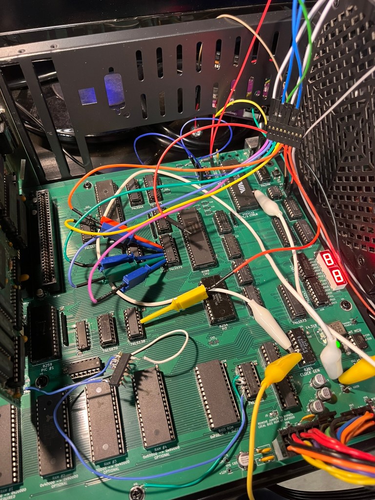
In the photo above, the spaghetti mess of cables is caused by both the breadboard fix for the de-multiplexers, and the logic analyzer I use to further troubleshoot the system. The error with the de-multiplexers stung more when I discovered that I had erroneously selected a 4-to-16 variant, meaning the 128KB of RAM I thought I had on this prototype was actually going to cap out at 64KB. That didn’t matter for the prototype, but it was still a reminder for me to pay better attention in the schematic design phase.
The 7-segment display proved to be invaluable for troubleshooting. Using a 4-bit latch proved to be a mistake, however, as 4-bit latches or registers were not easy to find in stock. Lesson learned – check the stock before you commit your design to a particular logic chip.
Most of the rest of the design worked exactly as intended. While I don’t have photos, I was able to use the pin headers exactly as intended to break out the necessary signals to another breadboard to test my keyboard controller circuits.
The prototype served its purpose: I was able to use it to test the core assumptions of my schematic and identify errors that needed to be addressed before making a full run of the much more complex motherboard I originally envisioned.
Interlude: The BIOS
To be able to do anything at all, my computer needed a BIOS. Given I was already building my own computer from scratch, the not-invented-here train had definitely left the station… So, of course I went ahead and wrote this myself.
I’m no stranger to writing low-level x86 code. I have spent a lot of time deep in kernel code for projects like the Pedigree Operating System. This time, there was no BIOS already present to depend upon! It was also a unique challenge to write BIOS code in that early environment, before it can even be assumed that RAM is functional.
The BIOS is 100% assembly code. I tried messing with the Digital Mars toolchain to write 16-bit real mode C, but ultimately found it easier to just write assembly code myself. I crafted some custom tools to help with generating the ROM images, but other than that I landed on a fairly typical NASM + GNU Binutils toolchain.
An example routine from the BIOS follows. There are around 3.5k lines of assembly at the time of writing this post.
int16_12:
    ; AH = 0x12 - Extended Get Keyboard Status
    push bx
    push ds
    mov ax, 0x40
    mov ds, ax
    mov al, byte [ds:0x17]
    mov ah, byte [ds:0x18]
    and ah, 0x73                        ; keep LCTRL, LALT, state bits
    mov bl, byte [ds:0x96]              ; grab extended bits for RCTRL/RALT
    and bl, 0x0C                        ; keep only RCTRL, RALT
    or ah, bl
    pop ds
    pop bx
    iret
To test that my BIOS was mostly on the right track, I took advantage of the popular Bochs PC emulator. I ran tests in two modes. The first mode, pictured below, used my BIOS as the main emulator BIOS, which helped flush out bugs in initialization that would be difficult to track down on the real hardware.

The second mode, pictured below, loaded my BIOS as an “Option ROM.” My code handled this case by avoiding all the system initialization procedures and simply overrode the BIOS system services instead. That allowed me to lean on the standard BIOS ROM to provide all the disk management and core functionality while I worked on getting my BIOS services to be compatible with MS-DOS.

This saved a ton of time. Being able to rapidly iterate with an emulator meant that every time I would load the BIOS on my computer, I had much more confidence that it would actually work. This also helped distinguish potential hardware bugs from software bugs.
While it’s never fun to have a session on my computer end due to a catastrophic software bug, every one of them leads to improvements that make future sessions even more stable. I don’t think too much about the software while I’m playing Civilization for hours on end without a fault, and that’s worth all the crashes and bugs to get here.
The Motherboard
Having succeeded with the prototype, I shifted focus to the first revision of the motherboard. This was going to be significantly more featureful compared to the prototype, and it needed to be! The goal was to run MS-DOS and a game, after all.
KiCAD is my design software of choice. This image is not the final layout but one of the early 3D renders of the motherboard during the design process.
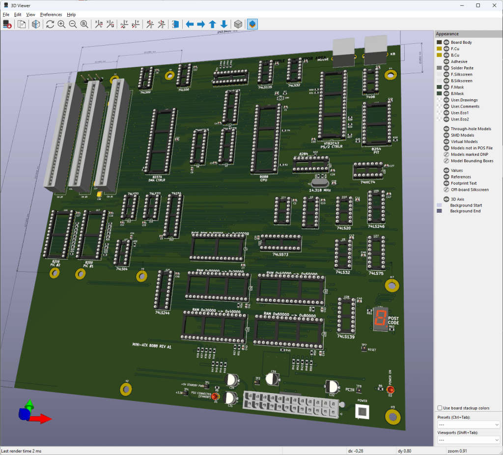
I ended up having JLCPCB manufacture these boards. These are 4-layer PCBs, and JLCPB’s pricing on 4-layer boards was very difficult to beat.
The first revision of the motherboard has a range of features:
- A basic system management controller using an ATtiny chip1 to handle ATX power signals and control the reset lines of the computer
- On-board PS/2 ports for keyboard and mouse
- 4 128K RAM sockets
- 1 64K ROM socket for the BIOS ROM
- 3 8-bit ISA card slots
- PC speaker connection
- Two 7-segment digit displays for POST codes and debugging
I elected to use surface-mount components for most of the resistors and capacitors that make up the design. All of the sockets, the ISA card slots, resistor packs, and PS/2 keyboard circuitry are through-hole components and require quite a lot of soldering. At this time, I also made the unfortunate discovery that I had erroneously flipped the footprints for the PS/2 connectors, making them unusable in this design. Alas – the next revision I build will have this fixed!
Here is a photo of the early board bring-up. The ATtiny in the bottom right was programmed and tested, and the rest of the motherboard was populated aside from just one chip that I missed in my original bill of materials.

Here, we have a few ISA cards in place – a Trident VGA card, and a serial/parallel interface card. Having a serial port proves useful for troubleshooting, especially if there are issues with the VGA card. The Trident VGA card is actually a 16-bit ISA card, but it autodetects an 8-bit bus and falls back to 8-bit mode.

Early on, I encountered some minor problems with the VGA card caused by a bug in the routing of the ISA bus READY line. ISA cards use this READY signal to extend the duration of memory accesses, allowing them to complete their own internal transactions if they are slower than the 8088’s normal memory access timing.
Having read plenty about CGA and its tendency to “snow”, I immediately recognized this kind of corruption as potentially caused by incorrect bus timing. Thankfully, I was right! In my schematic, the READY signal was going to the right place – the Intel 8284 clock generator chip. This chip takes care of generating digital clock signals and also generates the CPU’s RESET and READY signals. However, I misconfigured the secondary 8284 ready lines, causing it to always consider the bus as ready! A quick bodge to fix the misconfiguration allowed the READY signal to work again.
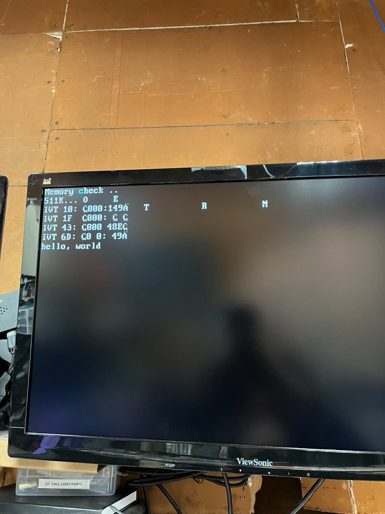
Hey – that’s MS-DOS! Yes, at this point the system was functional enough to make it all the way to the MS-DOS prompt. During early development, I left several BIOS services unimplemented and had them simply write to the screen. This let me make progress while still being able to track what was missing.

And finally, after all the fixes and patches, I was able to run Civilization on the computer!

What Bugs Remain?
I have one more revision of the motherboard that I’m preparing to produce. The current motherboard has a range of bugs – just look at all those wires! – and I would love to land on a completed design that doesn’t require quite so many bodge wires.
But what’s buggy?
Bug #1: DMA Controller
The DMA Controller was the controller that instilled the most fear in me during schematic design. It works by asking the CPU to completely release the bus, at which point it takes care of all the bus signaling. That means getting things wrong in the DMA schematics can lead to a totally frozen system.
Fortunately, while I did get it wrong, my mistakes don’t totally lock up the system.
The most significant bug I implemented in my schematic only appears during an actual transfer. 8088 CPUs generate a handful of control signals that my schematic converts into four overall signals to control the bus. These are IOR (I/O Read), IOW (I/O Write), MEMR (Memory Read), and MEMW (Memory Write). I made a faulty assumption that I could save some logic gates and use IOR/IOW to decide whether or not to enable memory. This works in general! However, during a DMA transfer that writes to system memory, the DMA controller will signal both IOR and MEMW. It does this because IOR will cause the device to generate data, and MEMW will cause that data to be written to memory.
That IOR signal is how a DMA transfer actually gets data from a device, so my attempt to optimize the gates backfired – IOR becoming active will disable all memory access, meaning the DMA is DOA!
My revised schematic fixes this by allowing IO and MEM signals to be active concurrently, using signals generated by the DMA controller to assist in disambiguation. I still have some testing to do with the DMA signals on the current motherboard before I feel confident getting the next revision manufactured.
Bug #2: PS/2 Port Mistakes
I have two major mistakes in my keyboard controller circuits.
The first major mistake is that I flipped the PS/2 port footprints on the PCB, which swapped the +5V power supply and the Ground pin. Thankfully, I have a resettable fuse on the power line for the PS/2 ports. This helped avoid causing problems elsewhere on the motherboard when I first plugged in a keyboard. It is an easy fix.
The second major mistake is that I forgot to place pull-up resistors on the output pins of the 74LS06 inverter chip that actually drives the signals to the keyboard or mouse. This chip is necessary to allow a single wire to carry bidirectional signaling between the computer and the keyboard, and without the pull-up resistors, neither device can correctly sense the state of the wire to know when it’s safe to transmit.
Both of these are fairly easy to fix in the schematic and the layout, but required a handful of bodges and extra soldering to fix on my first set of motherboards.
Bug #3: Incorrect Chip Selects
On PC-compatibles, the keyboard controller sits at I/O ports 0x60 and 0x64. In between those ports lies PC speaker control and a few other legacy ports. Ports between 0x70 and 0x7F include those used to control a real-time clock, if present.
My original schematic naively ignored most of these ports. That meant anything that tried to use the PC Speaker would send garbage to the PS/2 Controller, causing all kinds of problems with the keyboard logic. The revised design will use additional de-multiplexers to correctly distinguish I/O ports in this range.
This bug is actually the cause of the majority of the cable mess. I used an FPGA to implement the correct logic for port selection, which required connecting up signal lines, power, ground, and a 3.3V to 5V bidirectional level shifter as my computer’s signals all run at 5V. It’s messy. But without it, I won’t have a keyboard, and without a keyboard, I can’t achieve my goal of playing Civilization!
What Did I Learn?
I learned a lot!
- You’ll always find at least one error in your design moments after you submit your design for manufacturing (at which point, you can’t change a thing)
- Break out important signals to test points so they can be easily analyzed once the system is running
- 3D-print the PCB as a single-layer sheet to make sure every mounting hole is in the right spot (one of mine isn’t) – it’s cheap and fast
- Find ways to get feedback early. The 7-segment digits on both PCBs have been invaluable to track down problems that would have otherwise been invisible
- Use a ZIF socket for your BIOS ROM. It’s going to be annoying to keep removing it every time you make a software tweak
What’s Next?
Once I close out the next set of schematic revisions and get another set of motherboards manufactured, I’m sure I’ll find a few more issues that need attention. I’m slowly improving at this, but as you can see above – there’s still plenty of room for bugs to sneak in along the way. Fortunately, many of them can be mitigated with just some crafty wiring or a software patch.
The next revision will have a fifth RAM socket, so I can actually install 640KB of RAM. It makes a big difference!
I am also planning on adding an expansion header for adding ISA riser cards to the machine. Three card slots fit into my current design, and I don’t really want to make the PCB much larger for cost reasons. But three card slots isn’t a lot! I want to run my XT-IDE (for disk), Adlib compatible sound card, Trident VGA card, EMS memory expansion… you get the idea. I already have a basic design for a custom header and riser card that will allow me to add an additional 3-4 cards. Once I have the sockets in the design, the only limit is the size of the ATX case!
Once the next version of the motherboard is built and tested, I plan on releasing the source code for the BIOS and the KiCAD projects for the motherboard. I can’t promise that it’s the pinnacle of electrical or software engineering, but this computer ultimately achieves the goal I set for myself.
Hi
Could you send me the schematics? I’ve been wanting to make a simple but functional design for a long time.
I liked your design
I’ve uploaded the schematics here: https://github.com/miselin/M88